The Buck or Step-Down converter is an electric circuit that takes a higher input voltage and gives a lower voltage at the output, with minimal power loss. The function is detailed on Wikipedia but concisely, the converter uses a PWM signal to chop the input voltage and the result is fed to the consumer through a LC low-pass filter. This article lays out a quick application of the principle using a P-Channel MOSFET and an Arduino board.
The circuit
proposed here fulfills two main functions: chopping the input voltage and smoothing out the result. The first is done by the Q1 MOSFET which is power-opened by the Q2 bipolar transistor and passively closed by the R1 resistor. Last but not least, the L1 inductor and the C2 capacitor are forming with the consumer a RLC low-pass filter which attenuates the voltage ripple generated by the first function.

The device uses a flyback diode D1 that creates a path for the induced current to flow when the switch, Q1, is off. C1 capacitor acts as a near-by energy buffer that charges from the power source when the main switching transistor Q1 is off and discharges onto the RLC branch when Q1 is on.
The experiment
The schematics above omits the 15 volt input power source, the 8 Ohms consumer and the Arduino board generating the PWM signal. The Atmega164's pin 3 was chosen for providing the signal and here's the code behind it:
void setup() {
  // have port 3 generate a 8/256 = 3.125% duty cycle PWM signal
  analogWrite(3, 8);
}

void loop() {
  // nothing here
}
and the effect in Q2's collector:
 Wave shape in Q2's collector - a 96.875% = 1 - 3.125% duty cycle PWM signal, attenuated by a 1/11 factor
The PWM shape looks weird but it isn't. The signal in Q2's collector is the inverted version of the one generated by the Arduino. Let's now take a look at the signal in the Q2's gate. Expectedly, it should have the same shape.
 Wave shape in Q1's gate - a distorted 96.875% duty cycle PWM signal, attenuated by a 1/11 factor
It appears that the Q1 is not opened as fast as it gets closed. That could be explained by the fact that R2 is twice the value of the R1 and that the Q2 has a non-negligible ON resistance. Changing the R1 to match the R2 doesn't change the shape of the signal.
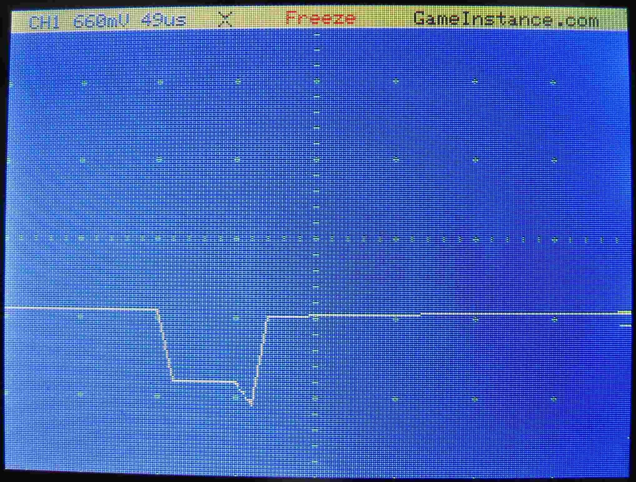 Wave shape in Q1's gate - a closer look at the distorted 96.875% duty cycle PWM signal, attenuated by a 1/11 factor
The MOSFET's gate charges just as fast as it discharges but it is the sudden closing of the Q1 that creates a small voltage overshot. The only explanation, at this stage, is that the parasitic impedances around the switching circuit are opposing the ideal propagation of the signal through the system. To counteract them, one should minimize stray capacitances and inductance and that in itself is another long story.
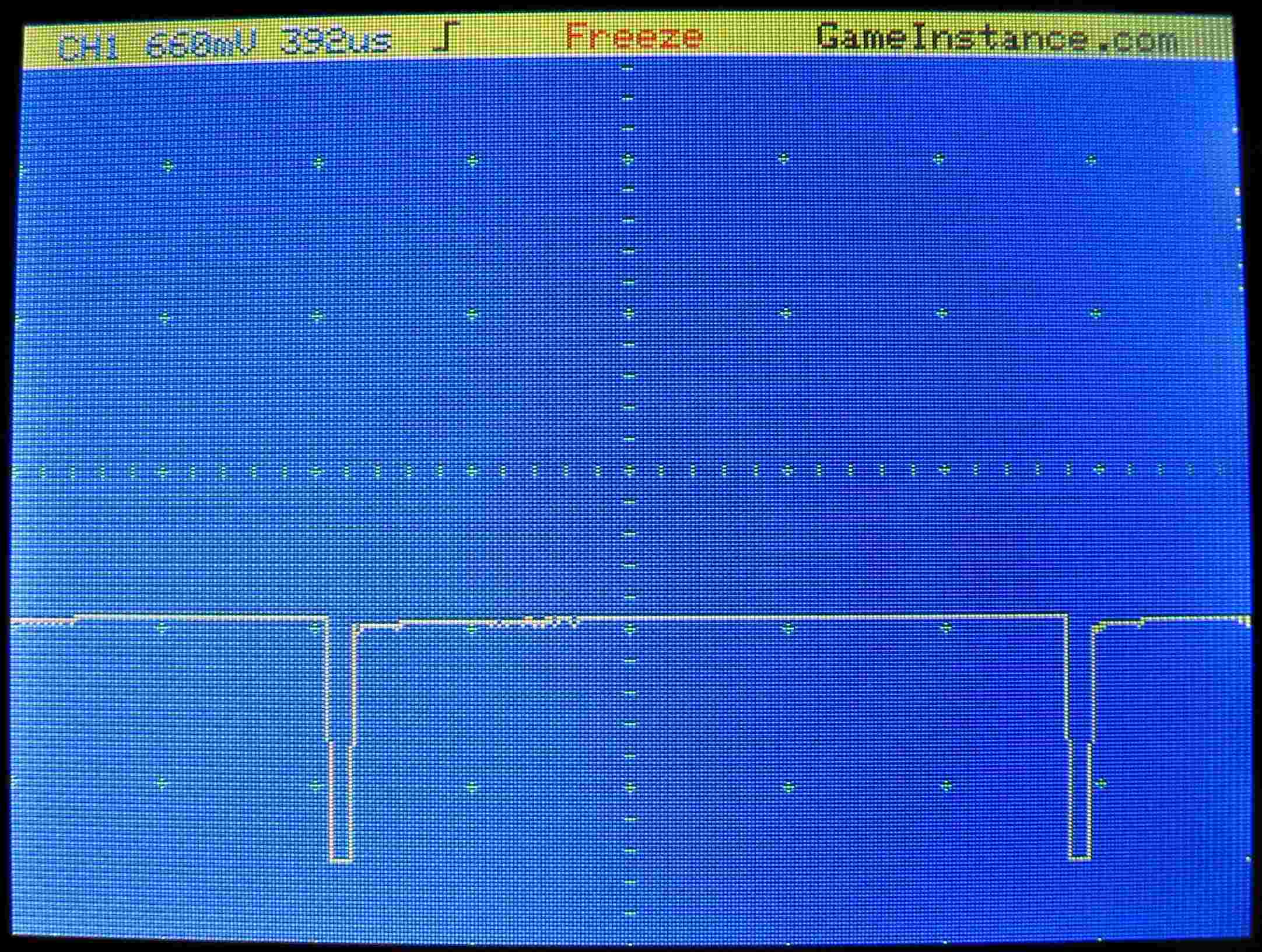
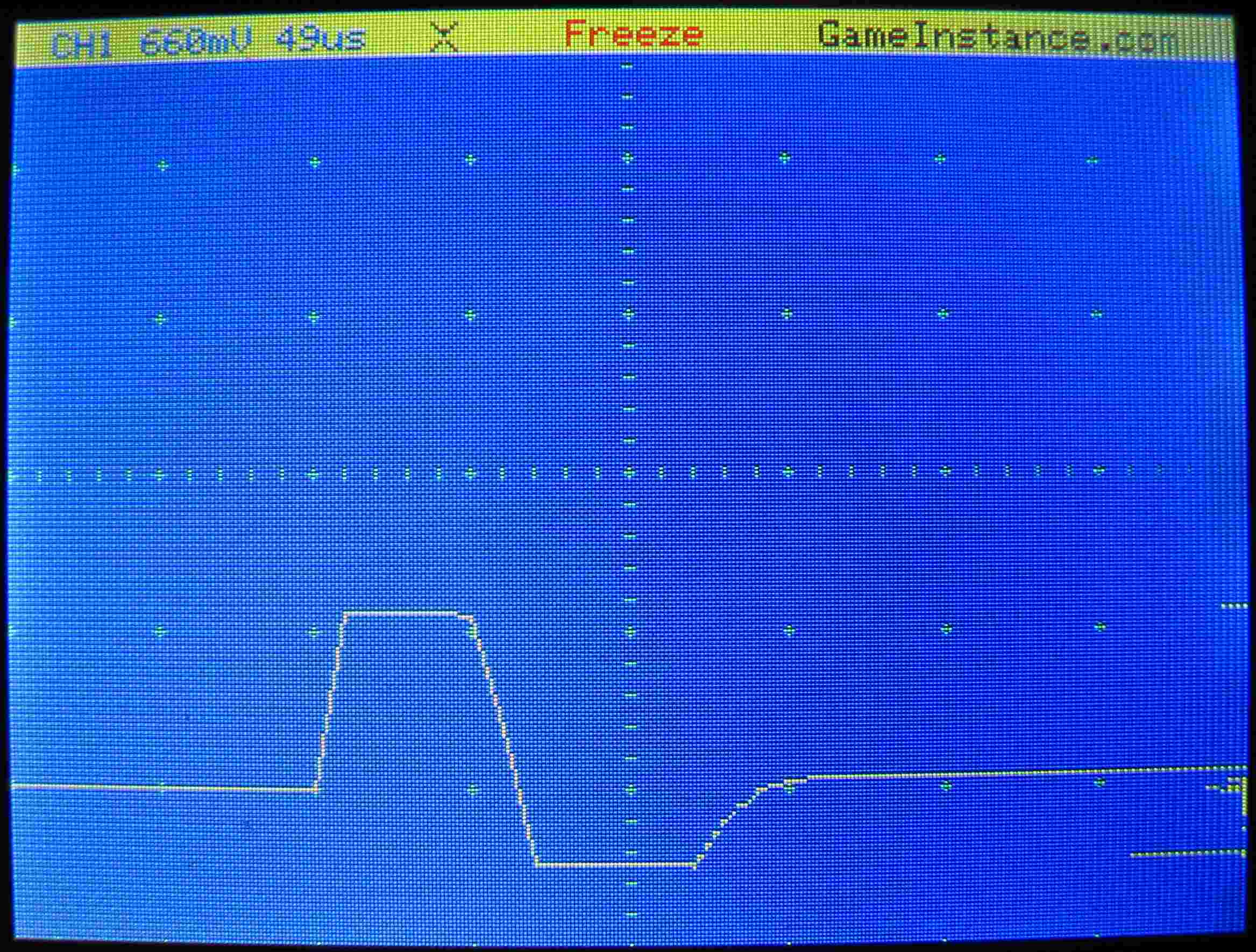
 Wave shape in Q1's drain - a distorted 3.125% duty cycle PWM signal, attenuated by a 1/11 factor
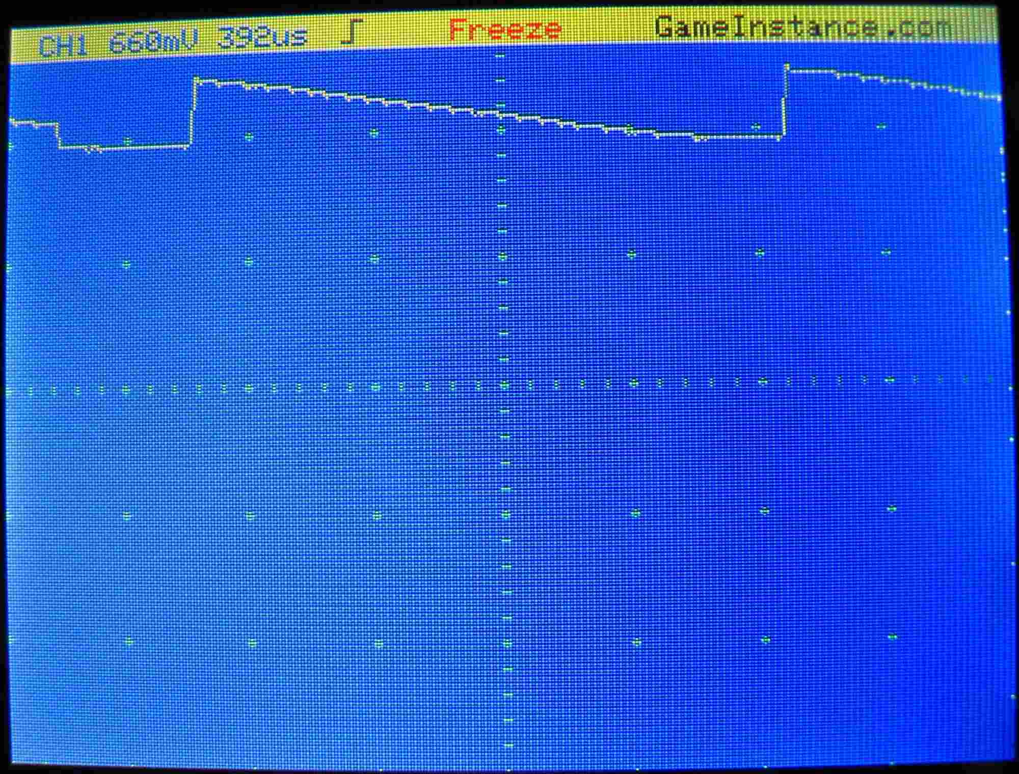
Probing the MOSFET's drain yields a new imperfect wave shape. The output of this stage should have been the amplified version of the PWM signal generated by the MCU. Instead, on the falling edge the signal drops below the zero level, remains at a constant level for a moment and then slowly gets back to zero. This is known as reverse recovery time and it is specific to diodes. The aforementioned is time given by the sum of the storage and transition intervals. Here it is again on a smaller time scale:
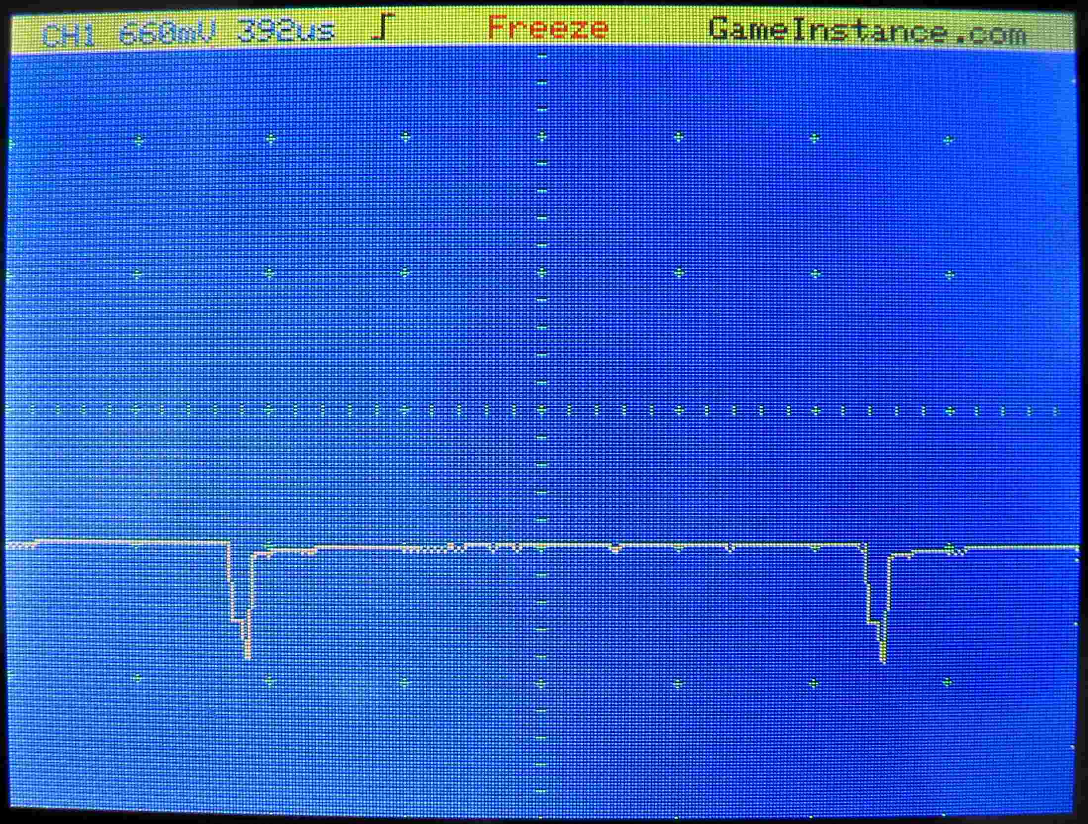
 Wave shape in Q1's drain - the rising edge, the falling edge dropping below zero, the storage interval and transition interval
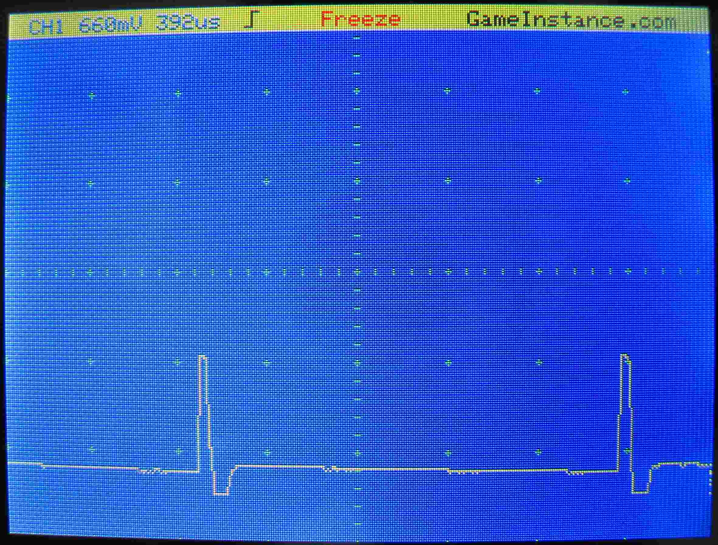
After the low-pass filtering stage a smoother signal is produced. The average value indicated by the voltmeter is 5.58 volts. The ripple picked by the oscilloscope is 0.8 volts.
 Buck converter output - averaging at 5.58 volts, ripple 0.8 volts, displayed after a 1/2 attenuation factor
Do excuse the marginal display issues with my oscilloscope. I made that tool myself not long ago. It has some bugs here and there.
The conclusion
One can and will obtain a functional buck converter: a circuit that reduces the input voltage via a PWM signal. However, breadboards are notorious for parasitic capacitances that, together with your setup's stray inductances, will ruin even a well calculated converter. If you're thinking of building a converter, even for testing purposes, do consider using a prototyping or a purpose-built PCB.
In the efficiency department, this configuration isn't a prize. The diode needs to be a Schottky with a quick reverse recovery time and low forward voltage drop. The switching frequency should be higher. The MOSFET needs to have quick rising and falling times and low capacitances. It should also be power opened and power closed, thus having a more evolved driving circuitry instead of the Q2. The input and output capacitors need to have low ESR and the list can continue. A good reference is the TI's Basic Calculation of a Buck Converter's Power Stage.
If you're not confident in your ability to design a buck converter or you lack the tools - a decent oscilloscope, a multimeter and a soldering station - you can always buy one that suits your needs. They're quite inexpensive these days. If you know your stuff and have at least a decent multimeter and the soldering tool, you can start with a dedicated buck converter IC and build your circuit around it based on the datasheet specs. You got the job done with minimum effort. No shame in that. For the rest of you getting the lay of the land to building switching power supplies, I hope this article helps you in some way. Do play around with various configurations but also read on the subject you've embarked on. I recommend Marty Brown's Power Supply Cookbook.