My previous article on Arduino controlled buck converter covered briefly the function and issues expected to be encountered with buck converters. Because of its inherent potential over conventional voltage regulators, I just had to make one myself. However, the design was limited by the components I had at the time and consequently had poor performance. This is a quantitative evaluation of its efficiency centering on identifying the main weak spots and how to address them.
Foremost
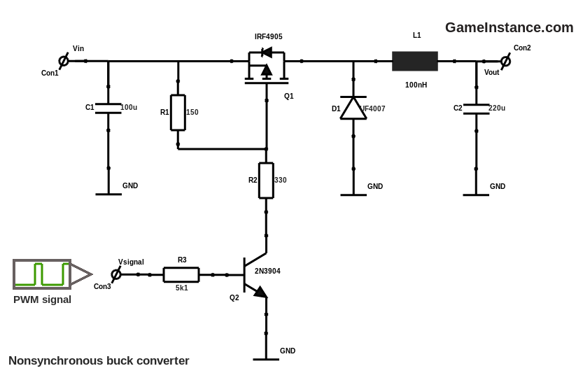
The circuit is known as non-synchronous because the built-up current accumulated in the L1 free-wheels into the consumer and back through a diode. The synchronous buck, on the other hand, uses a second power transistor instead of the diode that acts in sync with Q1 - it opens when the other is off - creating a stronger circuit path for that same current.
Evaluation rig
The circuit is fed by a 13.2V power source and the duty-cycle is incremented so that it outputs integer voltages from 1V to 12V onto a small 12V motor. Note that without a load, the circuit will output 13.2V no matter the non-zero duty-cycle. That's because C2 will charge in bursts and maintain the input voltage. Current measurements are made at the input and output giving the power figures Pin and Pout. The difference between the two gives the amount of lost power, Ploss.
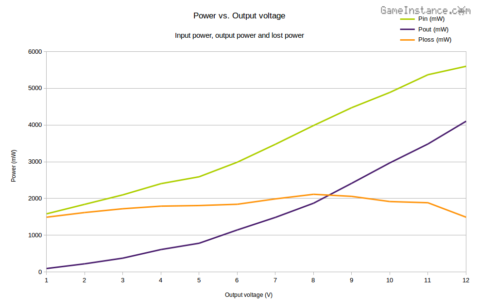
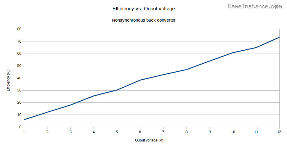
The dissipated power seems to start at 1.5W, spike at 2.06W and average at 1.8W. The efficiency chart shows values that are growing linearly with the output voltage. The first observation is that there is a steady consumer and a variable one.
So, which is which? Well, the prime suspects are D1 and Q1. We will look at the circuit driving Q1's gate and then at the L1-C2 low-pass filter. The switching frequency will be analyzed and some conclusion will be drawn.
Free-wheeling
diode D1 has a non-negligible forward voltage drop. The more it free-wheels, meaning low duty cycles, the more power is dissipated through its package. For the remainder of this paragraph we'll assume the system performs at the ambient temperature. While outputting 1V, the current settles at 96mA - which is also the current through the diode. At this current, the forward drop of the UF4007 is 0.87V, yielding a dissipated power of 84mW. Reasonable. Likewise, at 6V output the diode sees 190 mA giving a 1V forward drop, resulting in 190 mW power loss. However, at this output voltage the duty cycle is approximately 50%, meaning that the diode is producing that amount of heat only half of the time, averaging the loss to around 95mW. That's still 20 times less than the total.
It becomes obvious that the free-wheeling diode isn't the main energy waster, at least when used for small output currents. However, even this effect can be toned down by replacing the UF4007 with a Schottky, say an SS32.
The MOSFET
On paper it has virtually no voltage drop, IRF4905's can do 0.02 Ohms when fully on. This is great! However, this strength comes at a price. The MOSFET needs to be fully on and that means properly charging its gate, fast enough. Not charging it beyond the threshold voltage or spending too much time charging it are the main causes of transition loss in the MOSFETs.
In the circuit above, the MOSFET is power opened by Q2 via R1/R2 voltage divider and passively closed by R1. Assuming for now VCE=0V, we get -VGS=VIN*R1/(R1+R2)=13.2*150/480=4.125V. Looking in the MOSFET's data sheet we observe that the threshold voltage rating is -4V max. We're not yet in the clear because the conditions for that rating state that the voltage drop across it will be the same as the threshold voltage for a very small current of 250uA. Operating the transistor at VGS=-4.125V won't suffice. In fact the data sheet doesn't bother figuring the VDS/ID curve for a -VGS less than 4.5V. Unless VGS is around -4.5V, it is safe to expect massive losses at the MOSFET level. That can be obtained by slightly increasing R1 and lowering R2 values.
The driver
constitutes the current amplifying Q2 transistor. It's sole purpose is to open the MOSFET. It needs to withstand a maximum collector current of IC=VIN/R2=13.2/330=40mA. Its data sheet indicates a VCE drop of 1V at that current and a gain factor of 60x. With that in mind we get back to MOSFET's VGS which now becomes -VGS=(VIN-VCE)*R1/(R1+R2)=12.2*150/480=3.8125V, evidently below the rated 4V.
However, the Q2 will draw up to 40mA for charging the gate and 27.5mA for maintaining that voltage up. At VIN=13.2V the power dissipation within the driver is either P1=13.2*0.04=0.528W during gate charging or P2=13.2*0.0275=0.363W for maintaining the gate voltage. Considering the gate charging time negligible for now, we'd get an average power loss of P2*duty_cycle. At 6V output, where the duty cycle is expected to be around 50%, the power is P2/2=0.182W.
The MOSFET gate needs to be charged just like any capacitor up to a given value. For the IRF4905 that value is around 180nC. However, the input capacitance is also given CISS=3.4nF and we'll use that to determine the time taken to open the MOSFET. The most accurate formula to determine it is the following but can be approximated using τ=R1*CISS, which represents the time constant for the R1-CISS series combination. That gives 1.12us to raise the gate up to 63% of the applied 3.85V giving an insufficient VGS=2.43V.
The PWM frequency
fSW is influenced by the MOSFET's charging time. Ignoring the rated rise time, we observe that almost 10% of the signal period at 8kHz is occupied by the gate charge interval. This limits the duty cycle range from 10% to 95%. Anything outside that interval will cause unnecessary heat in the MOSFET. Lowering the PWM frequency would be the solution in this case.
We've seen how charge time influences PWM frequency, now let's discuss the effects of that on the rest of components in the circuit. The role of the L1-C2 filter is to minimize the ripple effect at the output. The lower the PWM frequency, the bigger values will be needed for the inductor and capacitor.
The capacitor
C2 is invaluable for averaging out the output voltage. Without it, there wouldn't really be a buck regulator. However, capacitors suffer from the equivalent series resistance, aka ESR. As the name suggests, a resistance will appear in series with the capacitor and it will grow with frequency. This is more of a problem for the electrolytic capacitors as they tend to generate ESRs of 2-7 Ohm. Ceramic capacitors are less affected but they're limited in capacity.
Conclusions
There is a concert of factors influencing one another and the performance of a buck regulator. Once you've mastered them, designing such a device would no longer be frustrating. Choosing smartly the gate charging voltage, an adequate MOSFET for the task, better free-wheeling diodes and low ESR capacitors will keep your design performance where it should. Here's a table briefing all the above in the descending order of their importance.
| # | Component | Parameter | Comment | Power loss in circuit |
|---|---|---|---|---|
| 1 | MOSFET | VGS | Must be few volts above the rated VTH. Below that the losses are sky-rocketing and unpredictable. | 1.3W |
| 2 | Driver | VON | Must be capable of delivering VGS > VTH. Ideally it should draw current from the power source only when transitioning the gate from VON to VOFF and vice-versa. | 0.363W * duty_cycle |
| 3 | MOSFET | CISS | As low as possible. Choosing a transistor with a small ID rating often yields smaller input capacitance. This lowers the time spent charging the gate and helps increasing PWM frequency. | 0.528W * gate_charge_time + 0.120W * gate_discharge_time |
| 4 | Diode | VF | As low as possible. Schottky diodes are rated at 0.4V for high currents. | 0.1W |
| 5 | Capacitor | ESR | As low as possible. A high ESR will increase the capacitor charge time and exacerbate the output ripple. Choose ceramic instead of electrolytic whenever possible. Low ESRs allow higher switching frequencies. | TBD |
| 6 | Diode | tRR | Reverse recovery time, as low as possible. Schottky diodes have virtually no tRR. Low tRR values allow higher switching frequencies. | TBD |
Note that the last column estimates the power losses for my circuit. It was only a guide in determining the order of priority.
I'll conclude - again - with the recommendation of proper documenting your project. Internet abounds with good sources. This article wasn't meant to give hints about what can go wrong and by how much, but also to help identifying the critical parameters that influence non-synchronous buck converters. From that you can expand your research and make better judgments.