This article covers the build of an oscilloscope using an 72MHz STM32F103C8 MCU packed on the famous blue-pill board and a 320x240 2.4" TFT NT35702 display. The device was constructed on single-side PCB that features 3 general purpose buttons and various extension connectors. The new an improved code employs DMA transfer between ADC and memory and uses FFT assembler implementation for power spectrum computing. Furthermore, it can export both the wave shape and its spectrum in a file on the SD card.
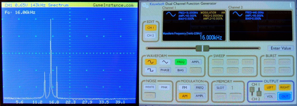 STM32 Oscilloscope - FFT spectrum representation for a test AM signal. Left - a screen capture of the oscilloscope. Right - the Android signal generator app developed by Keuwlsoft.
This was first prototyped about one and a half years ago. I was happy with the ADC sampling rate and resolution but I was using it in its original breadboard setup as I kept postponing a proper build of this rather inexpensive oscilloscope.
The build
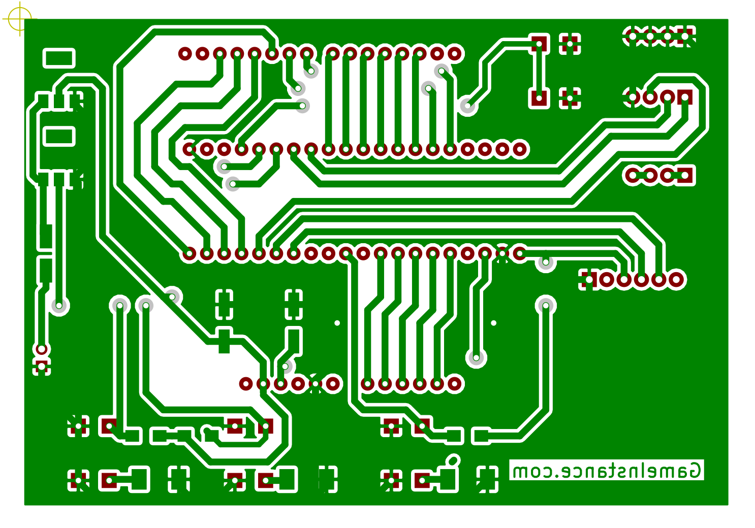
started as a KiCAD schematic, continued with the PCB routing, manufacturing and ended with soldering the parts. I placed the blue-pill in the middle of the PCB and the TFT headers in shield configuration around it. The funny thing is that I involuntarily ended-up creating a STM32 Arduino shield. To avoid physical contact between the blue-pill and the TFT, I had to solder the MCU board flush to the PCB and to heighten the shield connectors by approx. 1 cm. Also on the front side, I placed three buttons and four other header connectors. One of them interconnects the STM32's serial port via a FTDI232 controller to my computer. On the flip side, the board hosts two voltage regulators, satisfying the 3.3V and 5V requirements of the TFT and that's pretty much it.
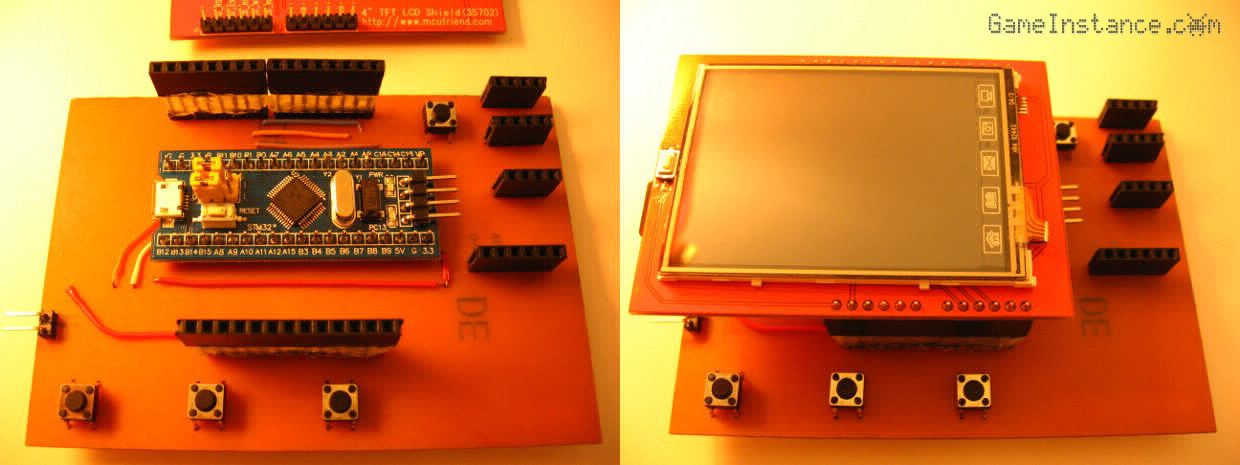 STM32 Oscilloscope - Observe the multi-purpose extension headers on the right-side of the board.
There are eight vias on the top layer that I could not avoid. They don't look too nice but serve the purpose. There's a reset button on the top-right corner for obvious reasons. The blue-pill board is covered by the TFT and so the builtin reset button is inaccessible. Also, to avoid handling the boot jumpers directly, I have created an extension three-wire cable with a three pin header at one end and a switch at the other. For further details on PCB creation, do check-out my previous article.
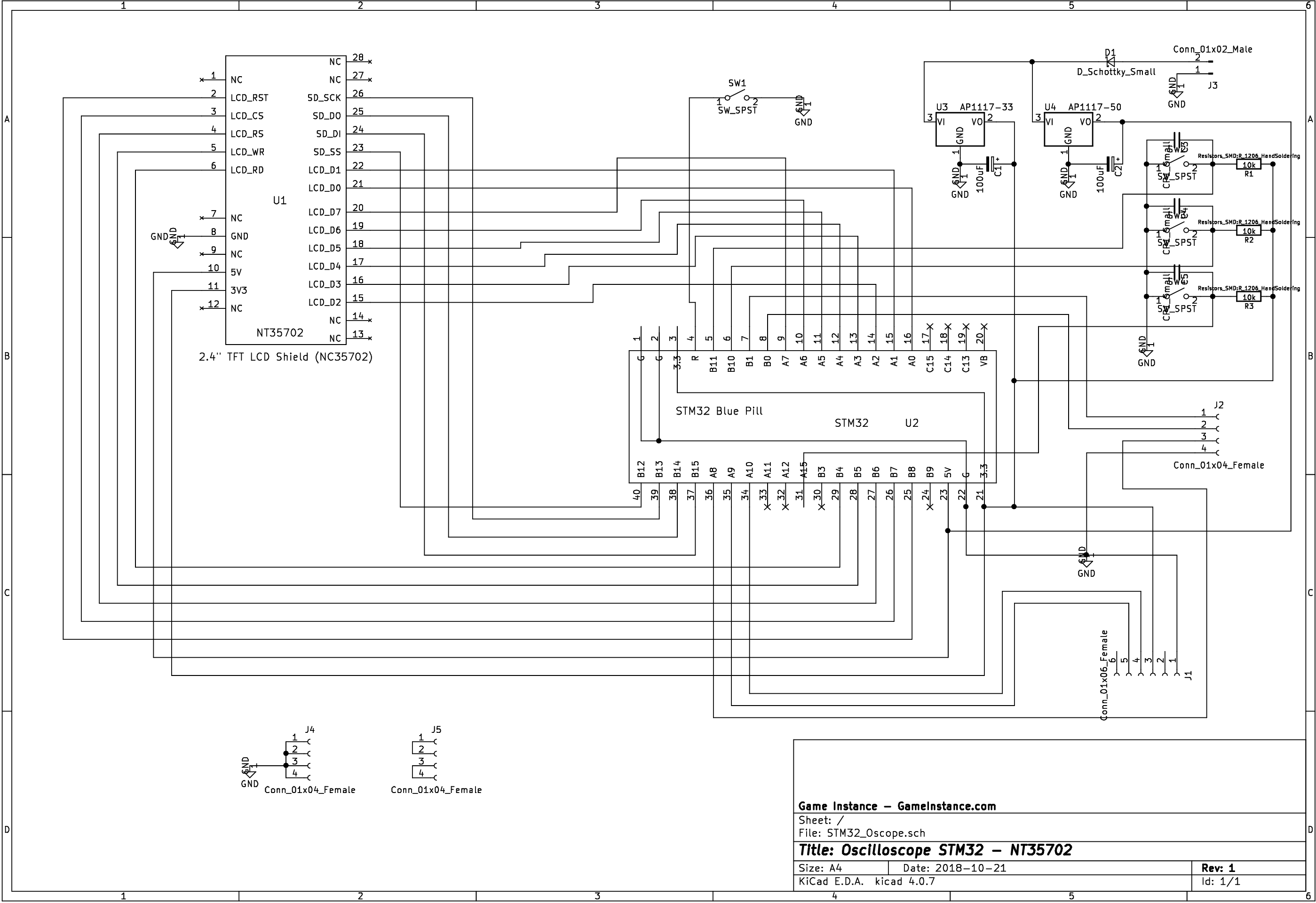
I moved from periodically probed button status to interrupt based button press detection. As a consequence I encountered what it's known as the button bounce phenomenon which manifests by apparent quick button press events before, after or before and after the actual button press. That is caused by an imperfect contact in the switch during on-off transitions and by the quick-to-detect MCU - the 72MHz clock frequency speaks for itself. The electronic fix for the high pulled buttons is the placing of a 100nF capacitor between the button signal line and GND. In effect this filters-out the switching noise and creates a smooth passage between high and low states.
I decided to throw a polarity protection diode in the schematic. This is always a good idea when you know you'll be spending some time handling the board.
The board does not include an input signal processing circuit. Instead there are a couple of female headers that break-out 2 analog inputs and one digital output. That gives a certain flexibility to the circuit permitting the addition of extension boards on top. One such board may contain an instrumentation amplifier and a voltage divider network or a 2-axis joystick and an extra button.
A lesson
learned, among other things, was to never again place logic signal traces in parallel with the analog input. I knew this would be a problem but I was constrained by space and other traces and I thought that a reasonable distance between the two would suffice. Apparently it doesn't. A fair amount of switching noise affects the input. To eliminate the problem I had to turn off the calibration signal. Anyway, in theory the analog and digital signals along with the corresponding areas below the MCU need to have dedicated power planes. Given my single-sided PCB design, I had to ignore this.
Check-out the next articles covering the STM32 oscilloscope code and box construction.