Little did I knew what I was getting into when I got this amp. I quickly found myself overwhelmed by its complexity, laborious disassembly, fragile boards and connectors, ribbon cables and some fancy mechanical switches. On one side I felt that I've been overly optimistic, on the other I was still confident in my ability to crack this. Several days into it and as the discouragement wore off, I started small, approaching it systematically. That led nowhere. But as I got acquainted with the design and the layout, I grew more confident. Realizing also I got nothing (more) to loose, I devised test setups that eventually gave useful conclusions. In case you're missing the point of this article, this is a follow-up on the defective Technics SU-VX920 I landed on.
This is not for the faint of heart. Read it at your own risk and peril!
The usual suspects
investigation is what I did first, even though it was obvious someone else tried that already. You can never overlook the small things. Besides, professional repair technicians can't afford to loose too much time on a repair and so it's probable they'd miss something. This amp is mine and I'm not in a hurry so I'll give it a bit more attention.
 Technics SU-VX920 - class AA field-effect MOS transistors
Hence, I looked for burned parts to find none. With no power, I started measuring all junctions, diodes and bipolar transistor but they were around the normal values (0.6 - 0.75V), except for zener diodes and some packages containing 2 diodes in series. Anyway, nothing was shorted or open. All field-effect transistors were OK but they were measured in-circuit, like the rest of the parts. Most of the ICs are dual operational amplifiers manufactured by Nec/Mitsubishi and all seemed OK (again, on the board). There's an 18-pin DIP Panasonic chip, AN7062, which is a souped-up operational amplifier, at the input of the amplification path. This was trickier to test because it's located on the hidden side of the front panel PCB, with pins accessible from the back. Nevertheless, this too didn't have clear symptoms of being defective. Of course, none of that means something isn't defective, it's just a way of eliminating the most common failure modes on semiconductors.
Warning:
Don't do any of this if you don't know what you're doing! If you still need to, think for yourself, understand what you're up against and don't follow blindly what you read, hear or watch online. Amplifiers run on voltages high enough to cause you harm!
Controlled power test
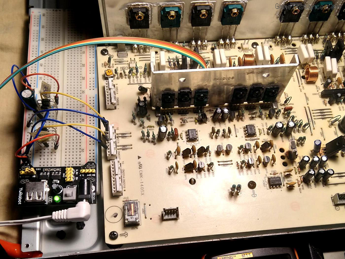
At this point I needed a way to power the amp without risking of damaging it further. According to the schematics, the amp is powered from two 62V DC rails and a low voltage AC coming from a low current secondary. The latter is required by the protection chip for a practical purpose, rather than safety. Luckily, I now have two HP 6289A power supplies so I can feed a sufficient 30V onto both rails, limiting the current to a safer 0.5A. With a small transformer I provided 6V to the AC presence pin of the AN7073 control and protection chip. Both the regulators and the AC transformer were connected to a multi-plug such that I could synchronize the power application. I butchered an old ATX power supply for the 4-pin connector to craft my test one, and that seems to do the trick.
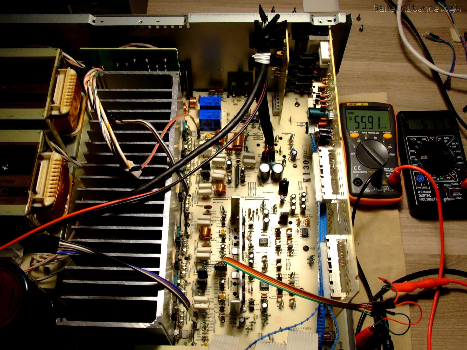 Technics SU-VX920 - controlled power supply setup and Dupont connectors on Test Points
The voltage control LED came online, unsurprisingly, but the current drive remained offline. That, according to the AN7072's sketchy datasheet (which is the nearest I could get to the actual AN7073 chip) meant one of two problems: overload or a DC component at the output. The first was excluded because the power supplies were indicating a very small current draw on both rails, apart for a transient at start-up. So, I was left to figure out the cause of the output DC offset, which was an unstable negative voltage between -24V and -12V.
A step back
It was clear to me that there have been attempts at repairing this unit and I wanted to investigate this lead. I also wanted to check the traces on the main PCB, clean the board and the main heat-sink. For this I had to disassemble everything.
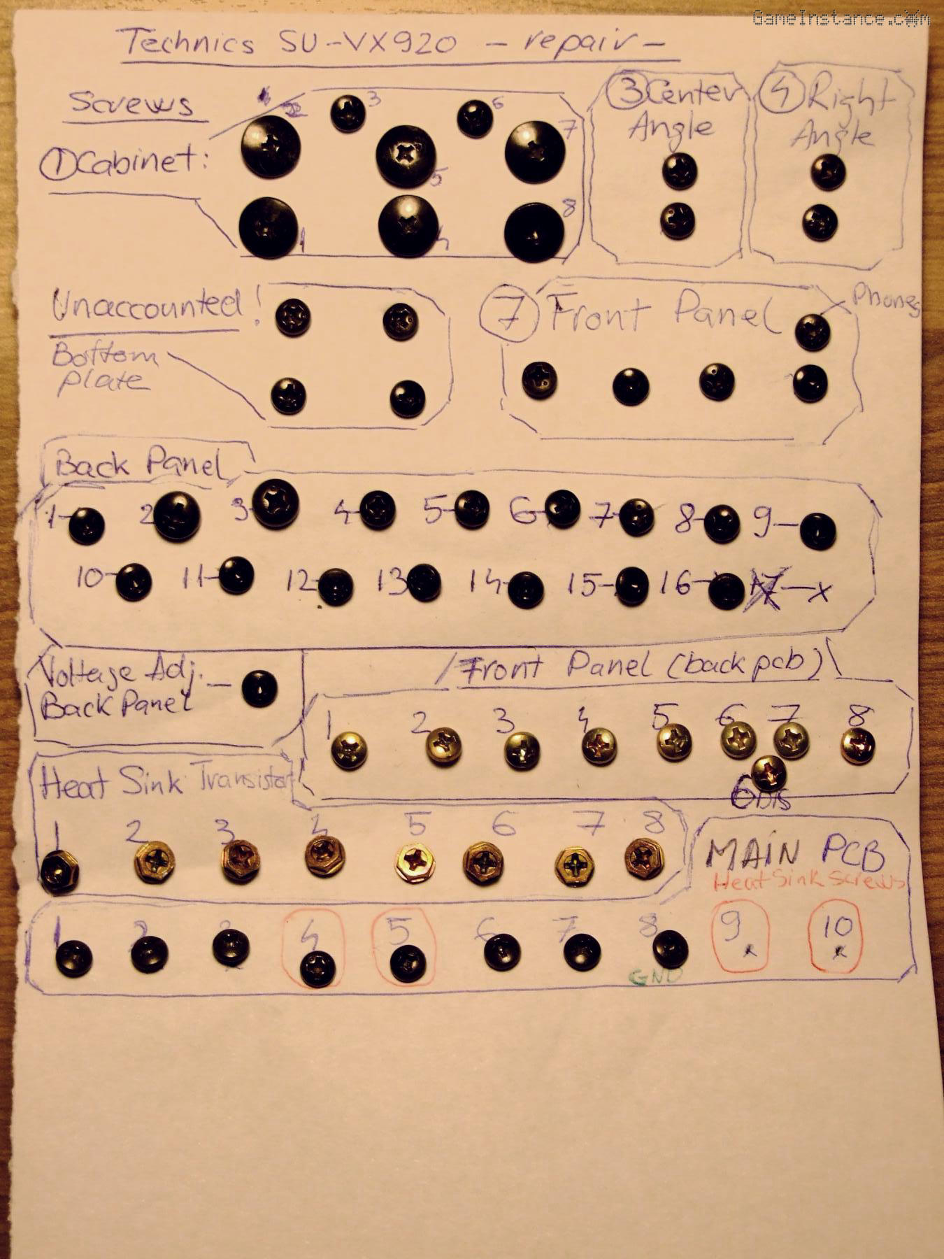 Technics SU-VX920 - screw organization
If I could briefly describe this amplifier, I'd say it is a complex machine. If you need to check the main board, you have to disassemble the entire unit and that sucks! OK, it has a servicing hatch on the bottom but that covers only a limited section of the main PCB, yet another bait for the technically inclined, much like the dual transformer thing. Nonetheless, I followed the service manual and removed the front panel, the back one, all auxiliary boards, the massive heat-sink and, finally, pulled-out the main PCB.
That said, I've seen hairier assembly/disassembly procedures.
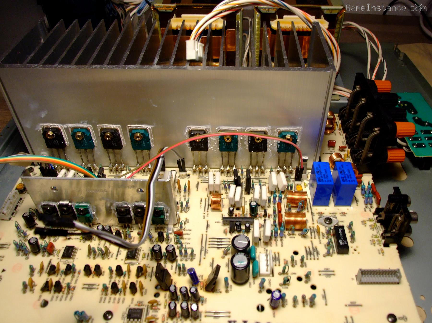 Technics SU-VX920 - main PCB, auxiliary boards removed
As I was expecting, the back of the PCB showed traces of systematic pull-test-resolder or replacement on several parts on a certain amplification channel. Lots of them! A decoupling capacitor seems to have been replaced, probably failed due to heat exposure considering its location nearby a regulation transistor Q651. Just like in the ST-S707, the continued exposure to heat has browned the board around that transistor which most likely caused exfoliation of the traces below it.
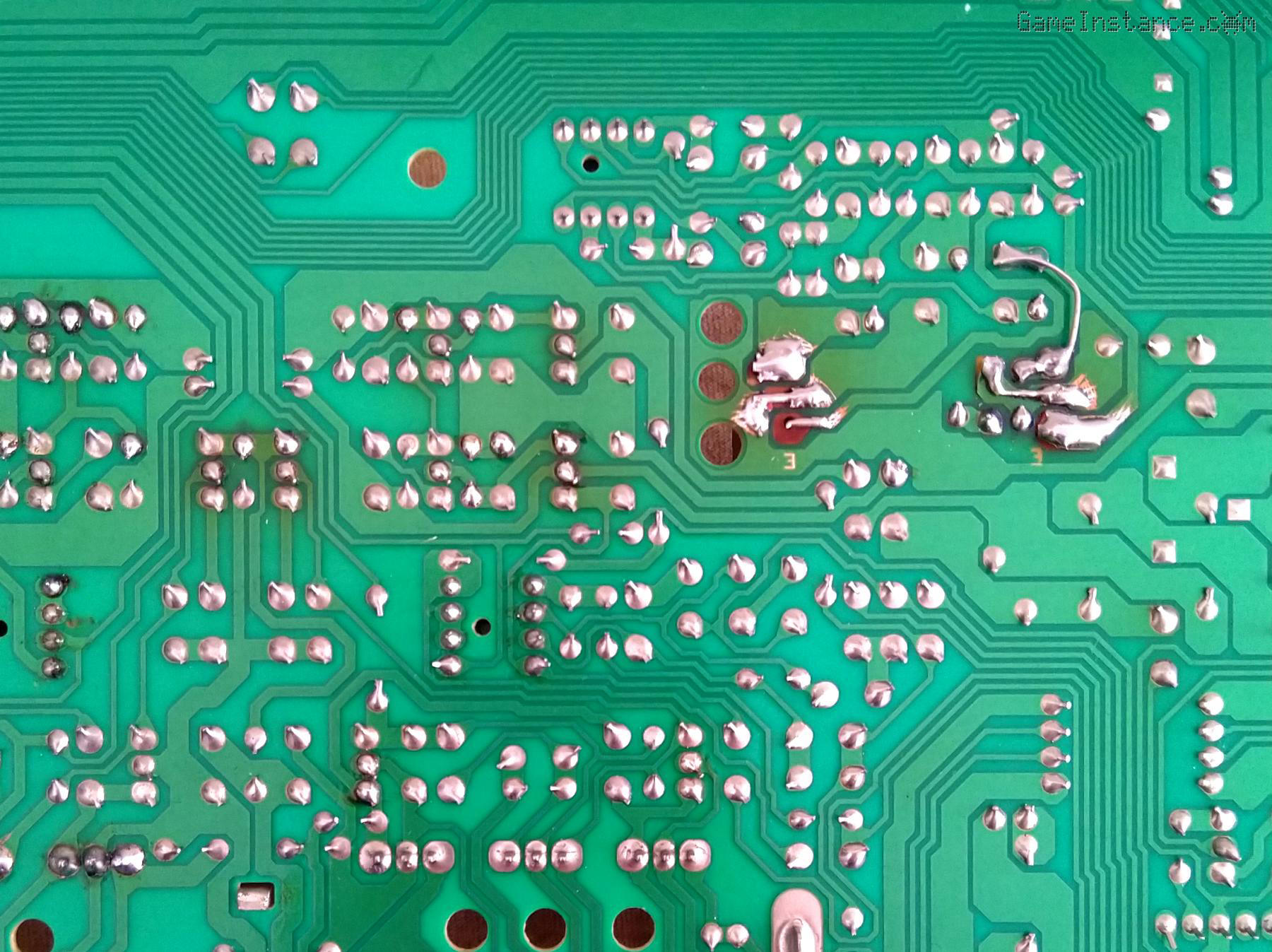 Technics SU-VX920 - main PCB, exfoliated traces and corrective hacks
And just like the SL-P200, this unit continues the Technics tradition for cold joints around the RCA connectors. It seems like the mechanical stress of assembly/disassembly and regular use has caused the brittle solder alloy to fail. This is a common problem on a large number of models built in the 80s and 90s.
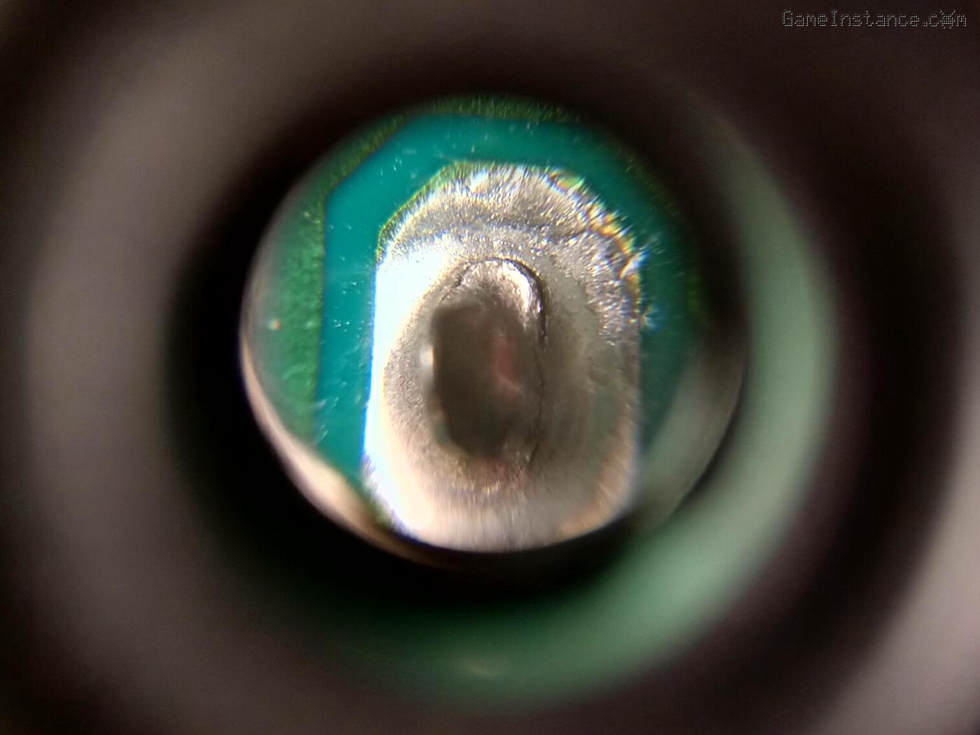 Technics SU-VX920 - input PCB, cold joint on an RCA connector
With the corrective hacks and cold joints fixed, everything was properly connected. Who ever worked on the main PCB did a pretty clean job and most likely knew what was doing. That made me have mixed thoughts about this unit, but mostly worry... I was starting to believe that it may have one of those ghost problems in which all parts are good but the system just isn't working. The previous owner may have lost his/her patience with it and then passed it along. And along it moved until it got to me.
Baffled, not
I didn't get discouraged and surely wasn't going to quit. If anything, I was intrigued. So I started to investigate the possibility of performing black-box tests on every board - most important being the main PCB. I was familiar with each module's function but I was lacking a good overall view of the system. The service manual schematic isn't quite clear in this aspect and that required some digging on my own.
What the service manual did provide was the static functioning point voltages along the amplification sub-modules. The signal is following a rather long path (for my taste), starting from the input PCB, passing through the main PCB, being pre-amplified and/or conditioned on the operation PCB, then back to the main PCB for more amplification. The input PCB wasn't hosting any critical circuitry, so I was confident I could remove it without affecting my test. The operation PCB was another story as it has the pivotal DC voltage amplification IC, AN7062. Although the output offset of that IC was dangerously high, around the 60V of the positive rail, the Q401/402 transistor was lowering it to 2.1V before leaving the operation board via the ribbon cable W401A/B.
 Technics SU-VX920 - black-box testing the main PCB
The 2.1V is roughly the drop on 3 junctions in series, so with a decoupled 5V supply, one 330 Ohm resistor and 3 general purpose diodes for each channel, I've breadboarded my test setup which I connected to the pin 5 and 9 along with the ground on the CN401A/B. Out of the 3 ribbons connecting the main PCB to the operation one, no other signal or offset is critical to the functioning of the amplifier. I enabled the 2.1V input, turned on the controlled power supply and ... nothing spectacular happened. No relay clicked, nothing fumed and the power supplies were indicating low currents. Reassuring! I then started probing the values along the signal path to notice that were all within parameters, as per the service manual, on both channels. Interesting! Furthermore, at the power amplifier output, before the master relays, the signal had near zero offset. Wow! I turned anxiously to the AN7073 protection chip to find that the control pin had a negative voltage, effectively opening the Q521 control transistor.
I instantly realized that the main PCB was seemingly in good working condition, at least statically. The fact that no relay was triggered, especially the RL503 connecting the output to the headphones jack, was still a mystery but not a huge problem at this point. A quick test showed that the relay coil had infinite resistance, likely from an interrupted winding. This test was the first breakthrough as it gave some confirmation and revealed a first bad part.
Confidence boost
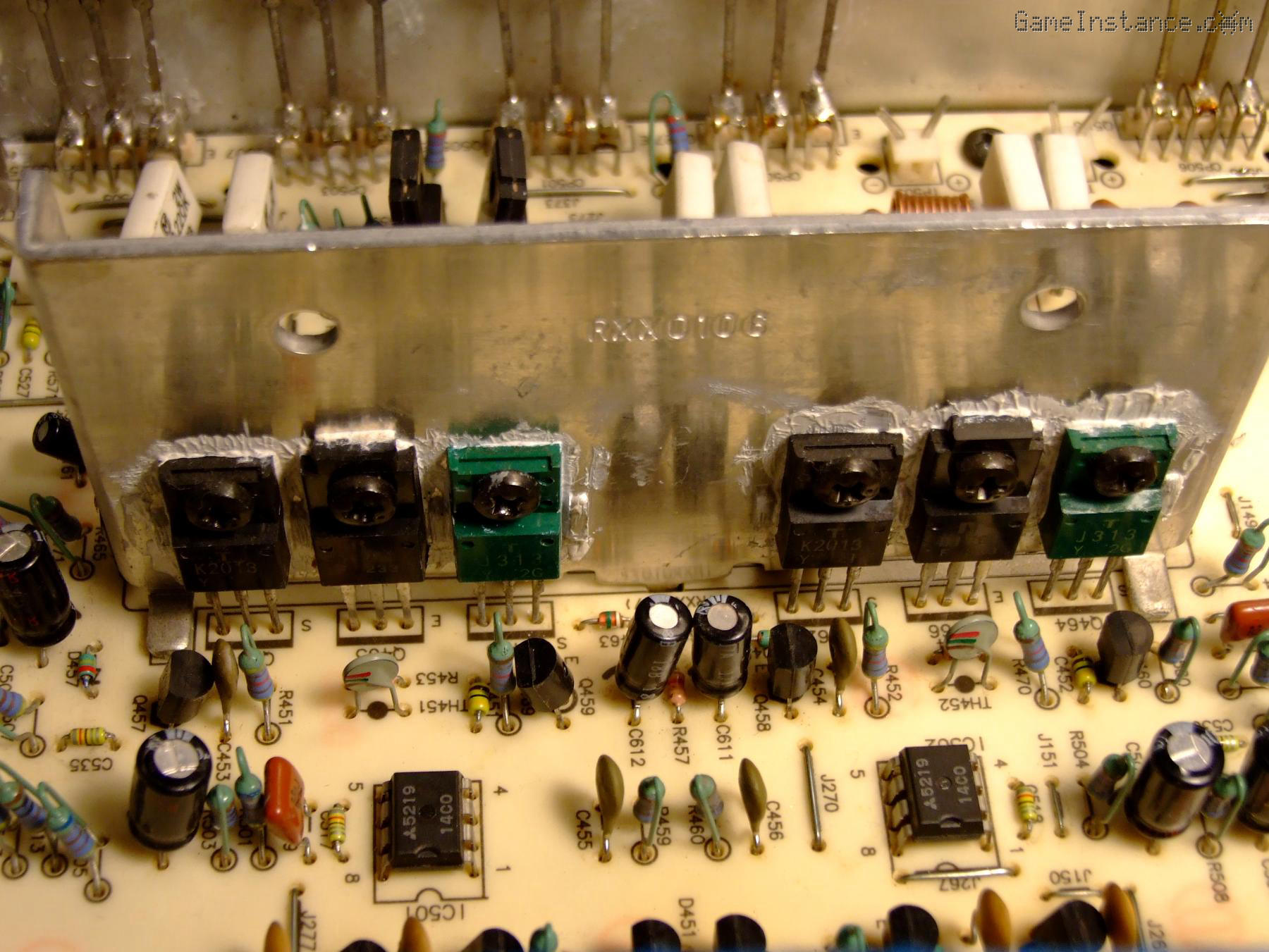
With some satisfaction from the previous step, I turned to the operation PCB which was hosting a lot of circuitry. Again, the entire front panel had to be disassembled to reach the parts and probe them easily.
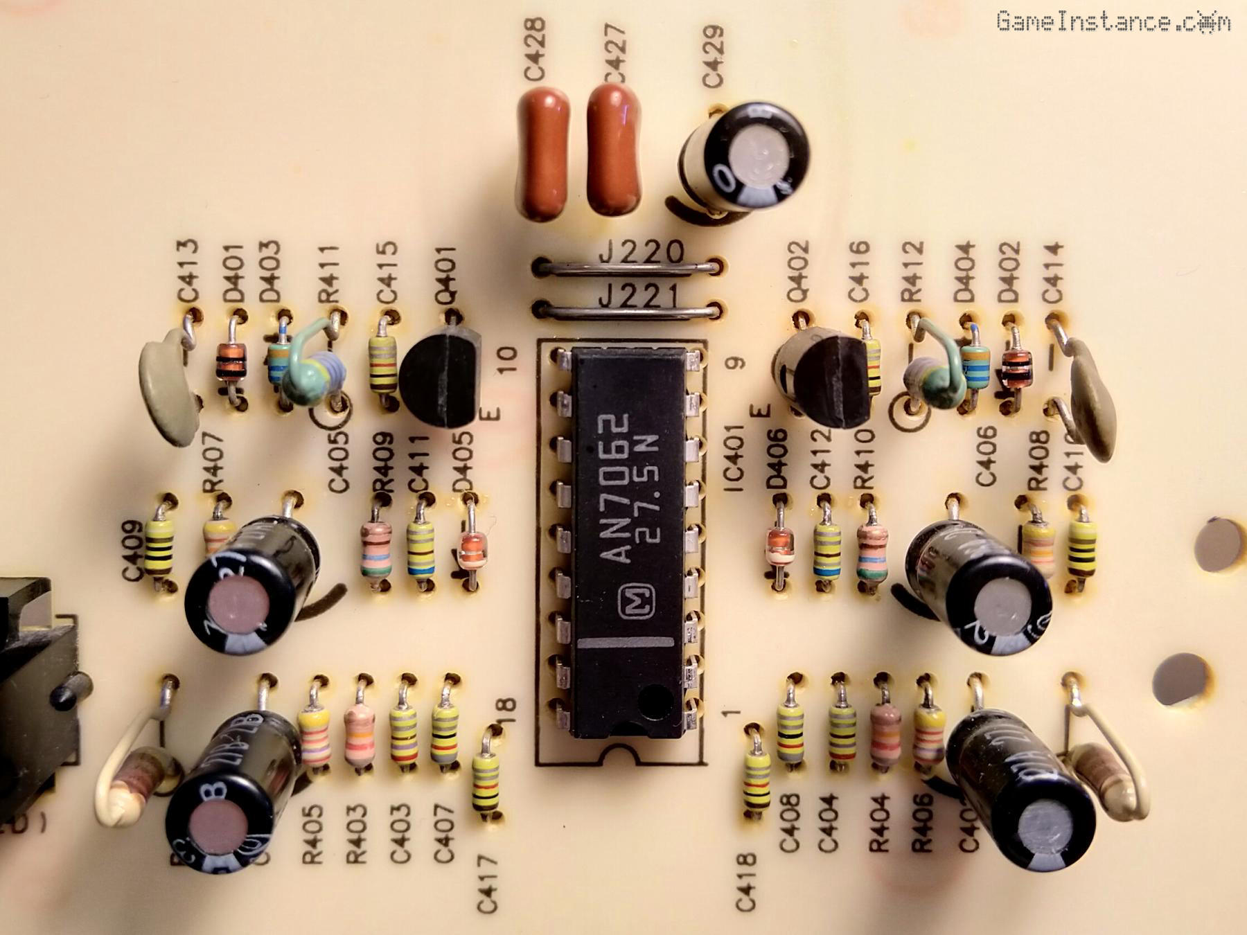 Technics SU-VX920 - voltage op-amp and adjacent circuitry on the operation PCB
The service manual shed some light onto how that works. Besides the power lines, the amplification part of the operation PCB has one input and one output per channel. The input is the system's feedback going into the negative input of the AN7062 while the output is the actual 2.1V offset signal. With a zero volt negative feedback (which is expected), and the positive input pulled to GND internally, the output gave exactly 2.1V. OK...
But WTF?!
If both modules essential to the amp are working, why isn't the amp? Why does it still have a DC offset at the output? This is exactly the proverbial ghost issue I was fearing. Something doesn't add-up!
Checking again components of working modules is futile but I found myself doing it anyway, to find, obviously, nothing out of the ordinary. The PCB connectors for the ribbons linking the two board have been pried-open rather brutally by others but they were still intact and functional. It's easy to get sucked into a vicious cycle, so I stopped again to reorganize.
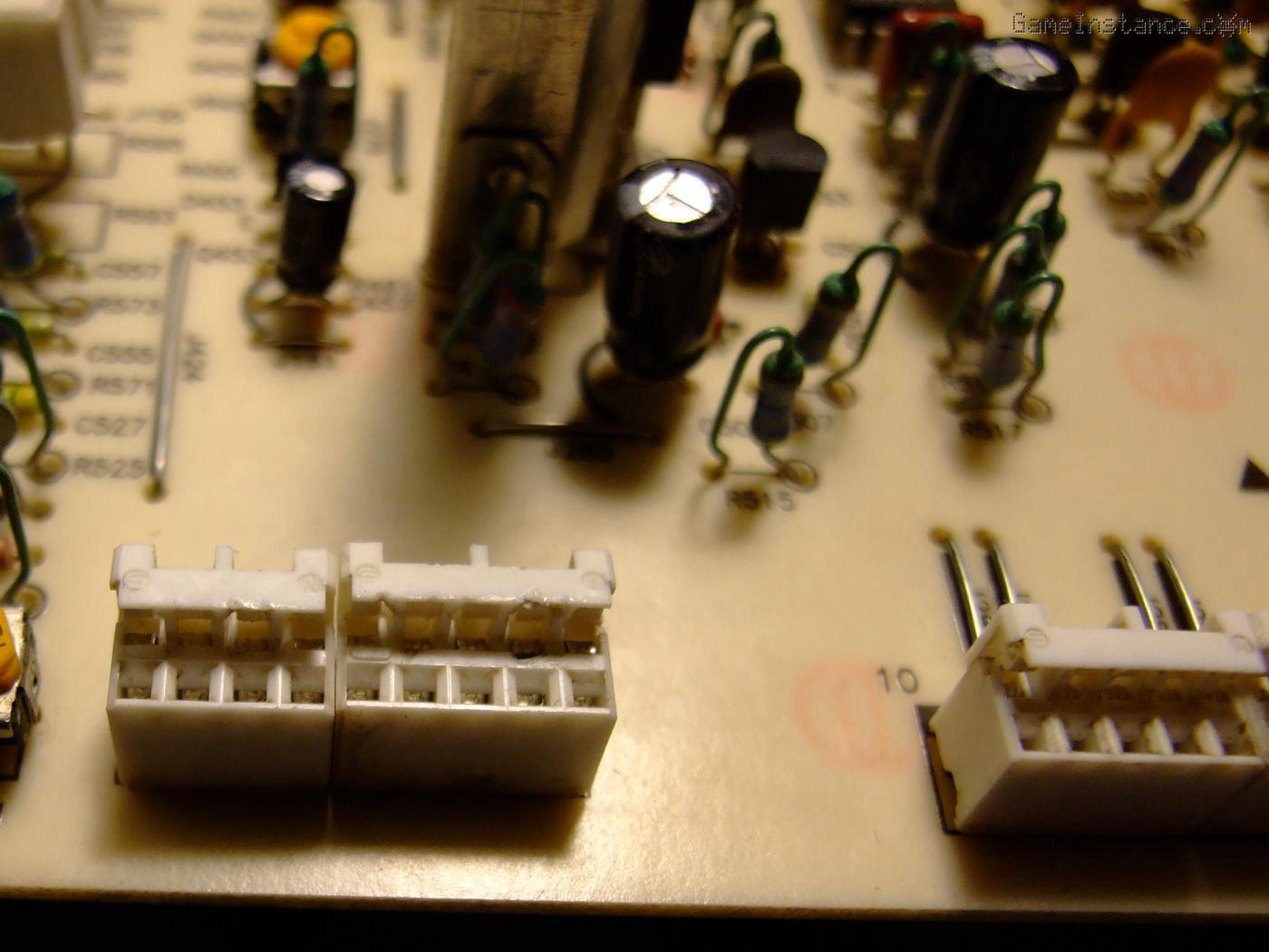 Technics SU-VX920 - forcibly pried-open connector guards, yet functional connections
Feeling something might be fishy about the inter-board connections, I bypassed them via a breadboard so that I get the ability to measure voltages and currents as well. Besides the DC offset all over the direct and feedback paths, one thing bothered me: the non-inverting input was around 4.4V vs the expected near zero. No outside source was pulling it up. Moreover, after the coupling capacitor there was a 82k pulling it to GND.
Down the rabbit hole
Usually, the voltage of a non-inverting input in an opamp is followed by the output in relation with the feedback network and voltage on the inverting one. That's an overly complicated way of saying that if the non-inverting input has 0, the output should too. Hmm! The idea of pulling the non-inverting pin to ground was forming but I was afraid what that might entail. So, I selected the mA scale on my multi-meter (one with a reasonably high internal resistance) and pulled it. The ammeter showed a transient, then zero. Consequently, the system output drops to 0.1V and few second later exits the protection mode. For the first time, both modules were working together but as a consequence of my hacky intervention. Some excitement and other questions rose.
This was weird. I could not understand why such a high impedance input could not be pulled-down by an 82k resistor. I tested R403/404 and they weren't busted. I tested the connections around them and there were no interruptions, no broken traces or cold joints. However, measuring the input impedance with the ground showed approximately 1MOhm, not 82 kOhm. I quickly realized that I was dealing with a grounding problem, hence the perfidious behavior. So, one pin of the 82k resistor was connected to its corresponding input, the other had no contact with the ground.
Pandora box
I knew at this point it was a matter of time until the cause of this grounding issue will reveal itself. After visually checking the traces on both PCBs revealed again nothing, it was time for another in-depth investigation. This opened another can of worms: the chassis ground vs. electric ground vs. signal ground. The rule of thumb says that if these need to be connected, that needs to happen in one place, and only one. That verifies as the main PCB has one screw connection to the chassis. This is coupled via C549 to the electrical GND of the system in the same point with the signal GND. This star configuration prevents ground loops and the deriving issues.
From that point on the PCB drawing, I started following all ground traces as they connected various components and boards. It is quite difficult to visually follow everything or to keep a mental note of what goes where. It wasn't until I started marking everything that I understood the grounding layout.
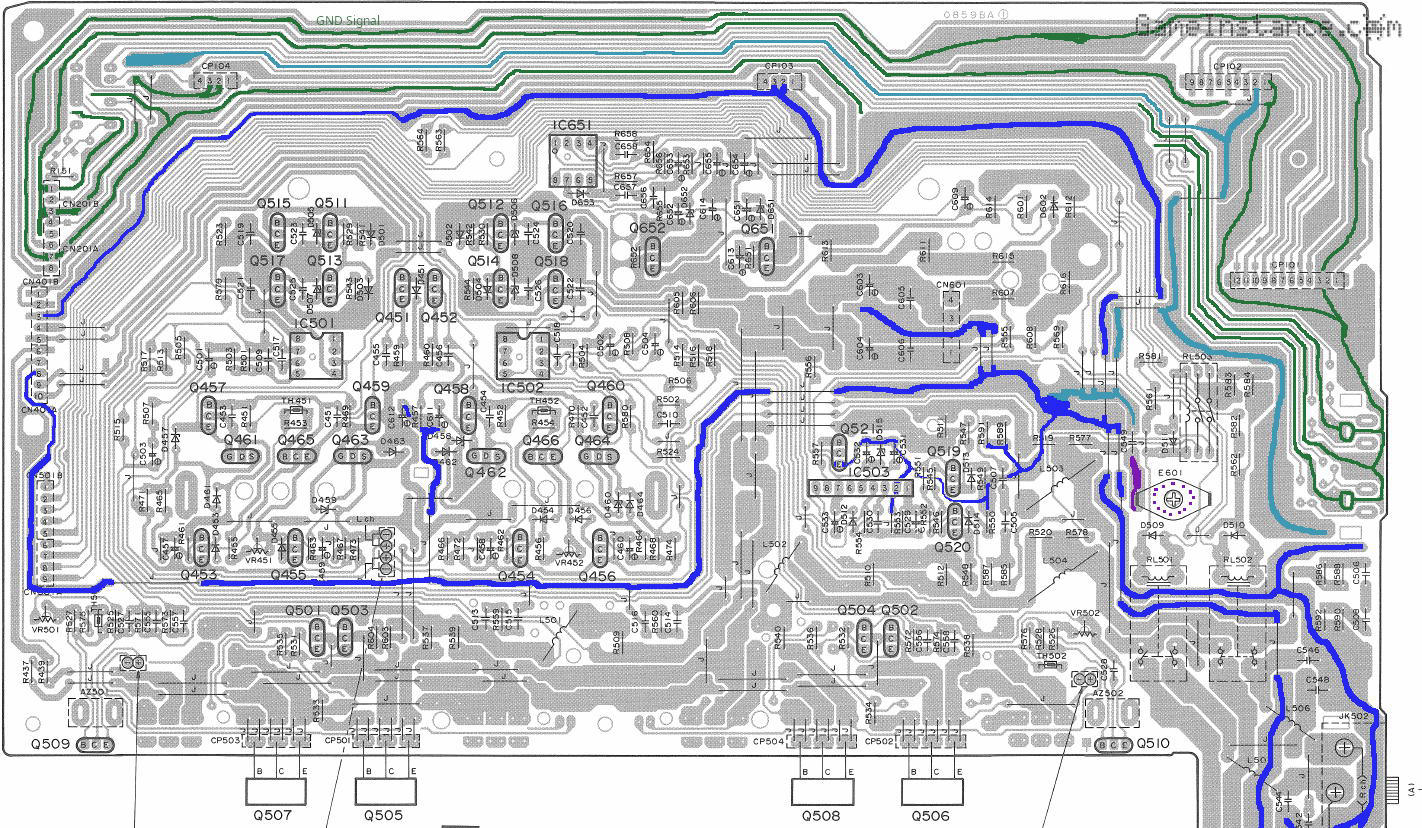 Technics SU-VX920 - main PCB grounding layout
What the schematic doesn't clearly differentiate is the types of ground and that's a major cause of confusion. However, if we're to follow the signals via the ribbon cable onto the CN201A/B connector, we can safely assume that the ground traces are the signal ground ones. If we're to look for CN401A/B we'll find supply lines, electrical grounds and amplification feedback. Basically the first cable carries high impedance signals while the latter, low impedance ones. If we're to analyze the PCB drawing of the operation circuit, we'll see that the signal and electrical grounds have no points in common, as expected.
Getting back to the main PCB, it becomes clear that the signal and electric ground do start from the same point but they are deliberately interrupted (see the lighter blue traces). The actual connection is made via the input PCB. Basically, without the input PCB inserted into its slot, the two grounds are disconnected, a DC offset would inherently form and the system won't function. That meant I tested everything wrong. But that didn't mean anything because the system with all its boards didn't work in the first place. Either-way, I plugged back the input PCB and, to no surprise, still no change. Bloody hell!
I knew I was up to something so I followed again the PCB design on the input circuit, to find that there was a huge island of copper connecting the pins 1 and 2 of the CN102 connector. Everything seemed in order: no cold joints or broken traces. Everything measured well. I got back to the main PCB to see that there were no such problems there either. At this point I started to believe my mind is playing tricks on me. With a screwdriver I shorted the two pins on the back of the main PCB and, obviously, the impedance between all ground types became near-zero. I carefully flipped the large and wobbly board to find the culprit... in plain sight.
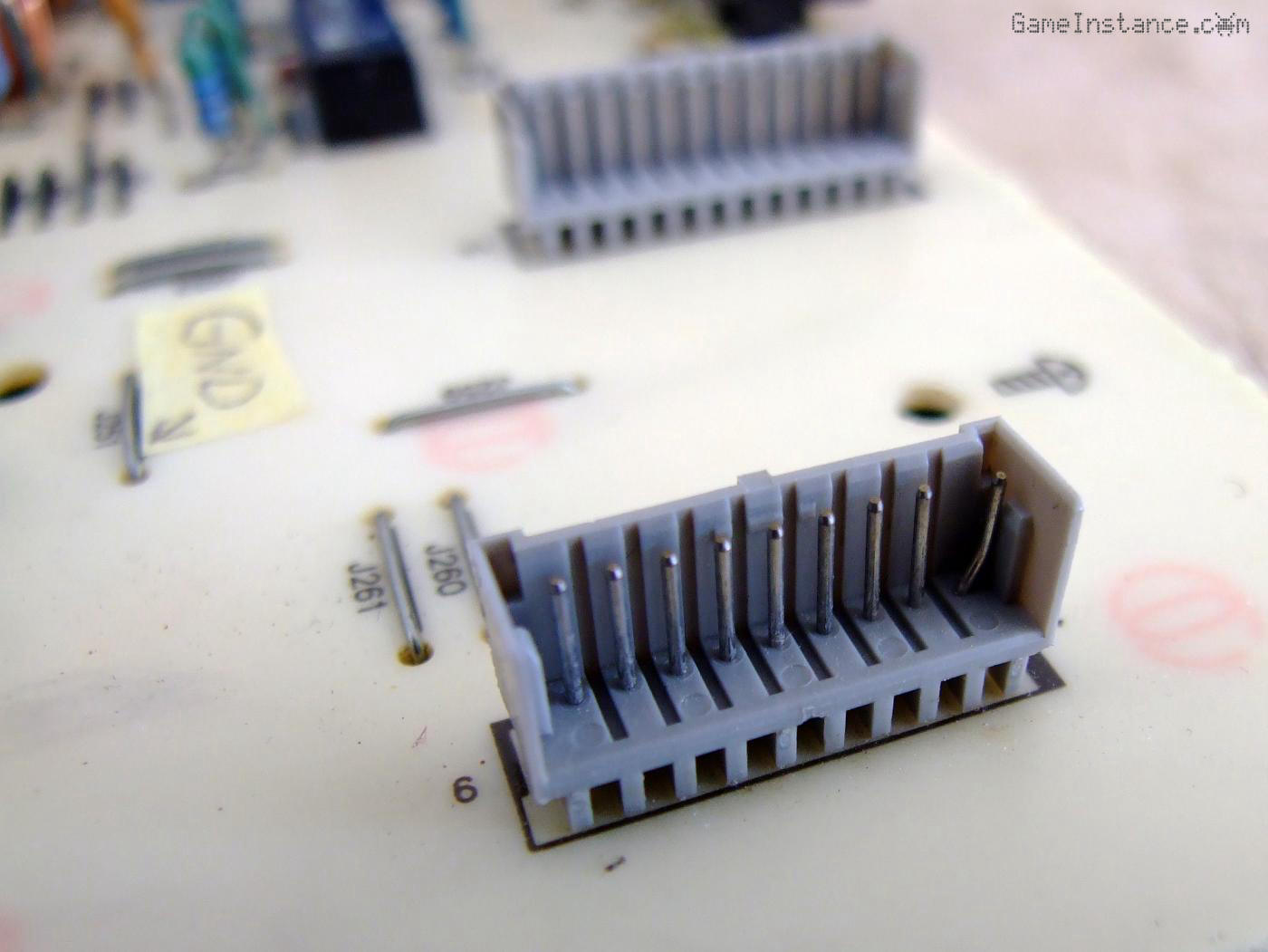 Technics SU-VX920 - main PCB grounding issue caused by a bent pin on the input PCB connector
It amazes me how many times I visually check those areas of the board without ever noticing that bent pin. It is also interesting how the input PCB even fit into that socket but I do remember noticing some elasticity to it, compared to other connectors of the same type. To my excuse, the location of the pin to one side was such that made it difficult to spot.
Let there be sound
And, with a straight pin and a correctly installed input PCB, the amp starts properly and engages the output drive. I was able to feed a sine at the input and view it on the scope at the output. I didn't connect the speakers or any other load as the transistors are still off the heatsinking piece. Anyway, I could not believe the actual cause was that simple.
From the looks of it and for some unknown reason, the previous owner had the amp serviced and, upon its reassembly, some careless technician must have forced the input PCB back into its slot. Probably did so without removing the back panel, as indicated in the service manual. With the small maneuvering space, the pin got pushed and then bent and that was it. This small mistake threw the entire unit into protection mode, never to be recovered... until today.
I'm still left with cleaning, reassembling, adjusting and testing the entire system. However, eager to put some music through it after the headphones relay adaptation, I came to the realization I was not done with this amp just yet.